Etched Emerges as AI Inference Specialist With $800M Backing and Custom Silicon
Etched Inc. has launched with $800 million in funding to build specialized chips for AI inference, differentiating itself from general-purpose processors by eliminating training circuits and adding performance optimizations.
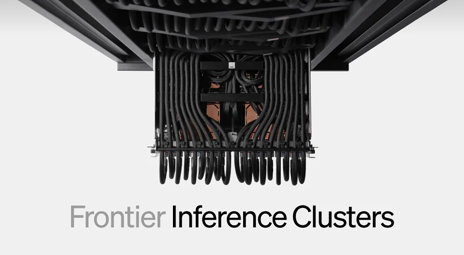
Etched Inc. unveiled itself today as an artificial intelligence inference chip developer backed by $800 million across multiple funding rounds. The company's most recent capital raise, completed in December, established a $5 billion valuation and drew participation from VentureTech Alliance, a fund connected to Taiwan Semiconductor Manufacturing Co., alongside more than a dozen additional investors including Geoffrey Hinton, Fei-Fei Li and Andrej Karpathy.
The startup will manufacture its inference processors on TSMC's N4P process node, an optimized variant of the company's five-nanometer technology that delivers 11% performance gains over the baseline version. Etched's initial prototype silicon completed production on TSMC's N4P line earlier this year.
Unlike Nvidia Corp.'s Rubin graphics processing unit, which handles both AI training and inference workloads, Etched's single-purpose approach allows engineers to strip away circuits designed for training. This architectural choice creates room to either cut power consumption or expand inference processing capacity.
Thermal Management and Performance Gains
Etched has incorporated multiple performance enhancements beyond its core design philosophy. A key challenge in GPU operation involves the relationship between computational throughput and heat generation: higher calculation rates produce more thermal output, which can trigger malfunctions beyond certain temperature thresholds. Conventional graphics processors address this through thermal throttling, a mechanism that reduces clock speeds as temperatures climb—a practice that degrades inference performance.
The company has engineered a proprietary technology designated LVI to minimize thermal throttling requirements. Etched claims its silicon can execute trillion-parameter AI models at 80%+ peak FLOPs while maintaining full clock rates, delivering substantial inference acceleration. The company asserts its chip achieves FLOP density—a performance metric—several times higher than competing AI processors currently available.
System Architecture and Deployment
Etched will distribute its silicon within a rack-scale inference appliance containing multiple chips mounted on proprietary circuit boards. The system incorporates custom cold plates, specialized metal components that transfer heat from processors into the rack's liquid cooling infrastructure.
Memory configuration combines SRAM and HBM technologies. SRAM, the fastest available RAM type, stores critical workload data on the AI chips themselves, while HBM memory provides substantially greater capacity at the cost of reduced speed. The appliance employs a custom interconnect enabling chips to access each other's memory through a shared system-wide memory pool that processes requests with lower latency than prior solutions.
Etched is currently scaling production and expects to begin shipping its first racks during summer. The company announced today that customer preorders have exceeded $1 billion in value.
Read more

Spotify Founder's Health Screening Startup Neko Brings Preventative Medicine to the U.S.
The body-scanning company co-founded by David Ek has arrived in New York with a 300,000-person waitlist and backing from nearly $1 billion in funding.
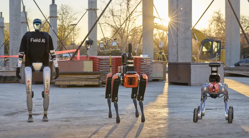
FieldAI Seeks $700M at $10B Valuation as Robot AI Demand Accelerates
The robotics AI startup is in advanced fundraising talks that would quintuple its valuation from last year, according to sources familiar with the matter.

Tech hiring slows even as employers post record open positions
A surge in IT job listings to three-year highs masks a contraction in actual hiring, with technology sector roles declining and unemployment ticking upward.